
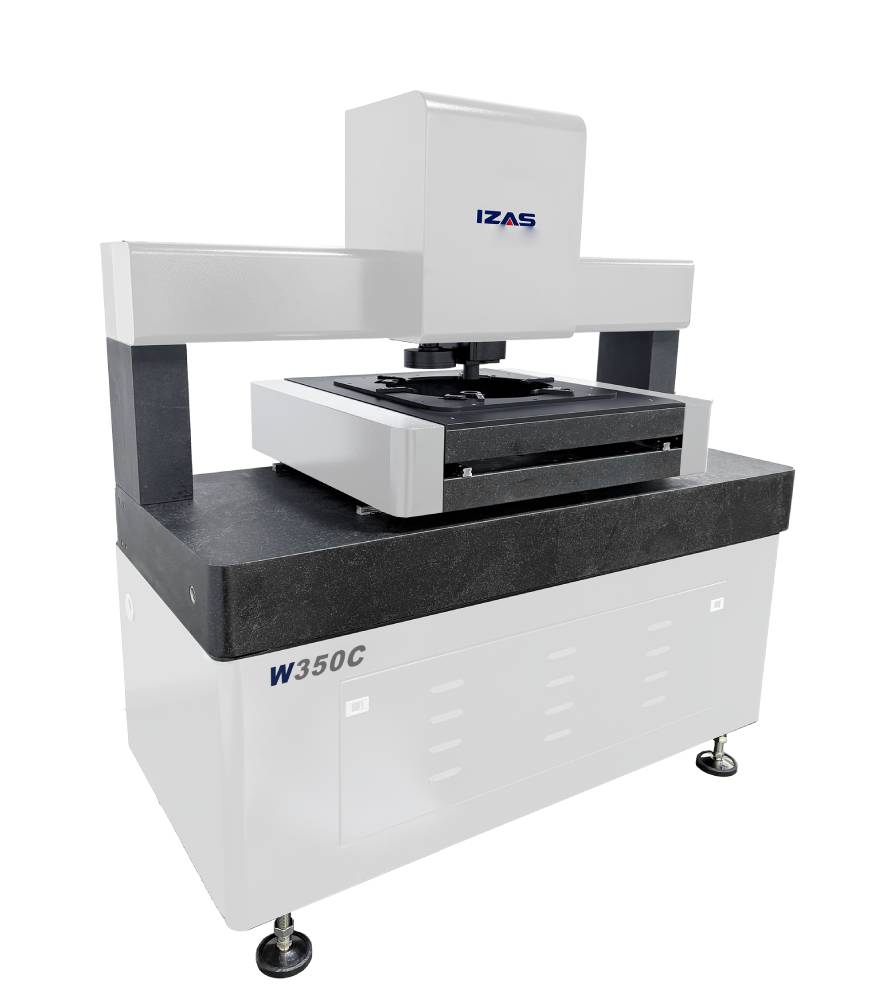

C-Series Wafer Thickness Measuring Machine
The C-series wafer thickness measuring machine adopts a measuring method with two opposite point spectral confocal displacement sensors (top and bottom). It is mainly used for measuring the thickness and flatness of wafers. Integrated with 2D vision measurement, it can detect 2D dimensions on wafer surfaces. Additionally, it is applicable to the thickness and flatness measurement of transparent/non-transparent films, sheet materials, and multi-layer transparent materials.
Product Features
-
Adopts point spectral confocal displacement sensors to achieve micron and sub-micron measurement accuracy;
-
Supports single-sided measurement and dual-sided opposite measurement. The opposite measurement mode completely eliminates errors caused by uneven bottom surfaces of workpieces;
-
Integrated visual imaging function to measure 2D surface dimensions of workpieces;
-
Supports single-point measurement at arbitrary positions and array scanning measurement with unlimited sampling points;
-
Adopts platform moving structure to ensure the thickness measurement accuracy of opposite spectral confocal sensors is not affected by platform displacement.
Software Features
-
Intuitive and user-friendly interface; one-click access to frequently used functions including measurement programming and operation control;
-
Supports the combined application of multiple sensors, including contact star probes, 3D line-scan lasers, point spectral confocal displacement sensors and line spectral confocal displacement sensors;
-
Built-in auto-focus, auto edge-finding and auto lighting adjustment functions. Combined with platform motion control, it realizes high-volume rapid measurement for products with identical specifications;
-
Supports auxiliary functions such as fast measurement via CAD file import, automatic code scanning and map navigation;
-
Enables measurement report export in multiple formats including Excel, PDF, Word and TXT, with a wide selection of configurable parameters;
-
Equipped with a comprehensive temperature compensation system, supporting two compensation modes: Temperature Mode and Proportion Mode, enabling rapid accuracy correction for diverse application scenarios.
| W350C Wafer Thickness
Measuring System |
Item | Specification |
| Overall Dimensions | Instrument dimensions L×W×H (mm) | 1430 × 740 × 1550 |
| Net weight (kg) | 900 | |
| Travel | Point Spectral Confocal Displacement Sensor: X / Y / Z (mm) | X: 350 Y: 350 Z: 100 |
| Imaging: X / Y / Z (mm) | X: 250 Y: 350 Z: 100 | |
| Measurement Accuracy | Point Spectral Confocal Sensor: static linearity accuracy (μm) | ±0.46 |
| Point Spectral Confocal Sensor: thickness measurement accuracy (μm) | ±2 | |
| Point Spectral Confocal Sensor: E UZ, MPE (μm) | ±(3.0 + L/200) | |
| Imaging: E UXY, MPE (μm) | ±(2.5 + L/200) | |
| L = length of the measured object, in mm. | ||
| Motion Performance | X/Y-axis speed (mm/s) | 200 |
| Z-axis speed (mm/s) | 150 | |
| Imaging System | Camera type | HD industrial digital camera |
| Resolution | 2 megapixels | |
| Optical System | Lens type | Continuous auto-zoom lens |
| Optical magnification range | 0.7X – 4.5X | |
| Image (display) magnification range | 18X – 230X | |
| Lens working distance (mm) | 90 ± 2 | |
| Magnification values are approximate; actual values depend on monitor size and resolution. | ||
| Illumination System | Surface light | LED cold light source, programmable brightness level |
| Contour light | LED cold light source, programmable brightness level | |
| Coaxial light | LED cold light source, programmable brightness level | |
| Encoder System | High-precision linear glass scale (μm) | 0.1 |
| Point Spectral Confocal Displacement Sensor | Working distance | 36 mm |
| Effective range | ±1.15 mm | |
| Static linearity accuracy | ±0.46 μm | |
| Dual-head opposed / single-head transmission thickness accuracy | ±2 μm | |
| Measurement modes | Displacement mode: flatness, warpage, height difference, etc.
Thickness mode: direct-penetration thickness measurement of transparent materials Opposed mode: dual-sensor opposed thickness measurement |
|
| Motion Joystick | High-performance configuration | LCD display for real-time monitoring of machine status; one-touch emergency-stop button for safe operation; speed-adjustment knob for flexible motion control |
| Industrial Computer | High-performance configuration | Intel i7 processor • 16GB DDR4 RAM • 1024GB SSD • 27″ HD LCD monitor • Windows 10 OS |
| Worktable Load | Load capacity (kg) | 5 |
| Power Requirements | Voltage | AC 200–240V, 50/60Hz |
| Power consumption | ≥1500W | |
| Grounding | Mandatory; ground resistance ≤ 4Ω | |
| Operating Environment | Temperature range | 20 ± 2℃ |
| Temperature gradient | 0.5℃/h, 2℃/24h | |
| Relative humidity | 30%–80% | |
| Vibration level | < 0.002g, below 15Hz, away from vibration sources | |