
Choosing a wafer thickness measurement method is not about which technique is “most accurate.” It is a matching exercise: does the wafer transmit light at the sensor wavelength, must you resolve individual layer interfaces, what throughput does the line demand, can your site hold the environment the instrument needs? Three non-contact approaches dominate every shortlist — capacitive, spectral confocal and interferometry. This article compares them as a buyer should: by application boundary and integration burden, not by a headline resolution figure.
Why non-contact wafer thickness measurement is the default
Contact gauging still serves offline verification and opaque samples. But once wafers are thinned, the probe tip brings risks no fab wants: surface marking, particle generation, micro-cracking. Non-contact measurement then stops being a preference. All three methods below qualify.
Method 1: Capacitive gauging
Each side of the wafer gets a probe. Each probe measures the electrical gap to the surface it faces; subtracting both gaps from the known probe separation gives thickness, and scanning builds the TTV, bow and warp map.
The technique is indifferent to whether the wafer transmits light, and needs no refractive index to convert an optical reading into a physical one. Its limits are equally structural: it reports total thickness only, cannot separate layer interfaces, and is sensitive to the dielectric properties of any film on the surface. It suits bare or lightly processed wafers better than patterned or coated ones. Take performance figures from the datasheet.
Method 2: Spectral confocal — one optical head, three measurement modes
A spectral confocal sensor encodes axial distance into wavelength: broadband light is dispersed so each wavelength focuses at a different height, and only the wavelength returning through the confocal aperture reaches the spectrometer. The peak wavelength maps directly to surface position — and because the returned signal carries the reflection from every interface the light reaches, one sensor resolves more than one surface, which is what makes thickness measurement possible without touching the part.
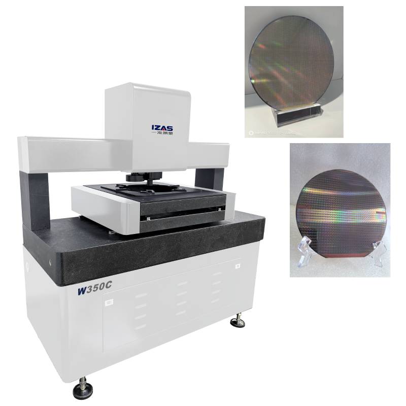
Like our W350C is built on this principle and does not restrict you to transparent material. Three modes:
- Displacement — flatness, warp, height difference.
- Thickness — one sensor penetrates transparent material, no surface preparation.
- Opposed — upper and lower sensors together, for material light cannot pass through, semiconductor wafers included.
That third mode is what buyers miss. Spectral confocal is routinely filed under glass and transparent films; with two opposed heads it covers opaque semiconductor wafers too.
Specifications: 36 mm working distance, ±1.15 mm effective range, ±0.46 μm static linear accuracy, ±2 μm thickness accuracy, against a length-dependent limit of ±(3.0 + L/200) μm. It handles 4, 6, 8 and 12-inch wafers and reports thickness, TTV, bow and warp. Travel is 350 × 350 × 100 mm (Z customisable), with 0.1 μm grating scales and grating-pulse-triggered scanning at 200 mm/s in X/Y, on an FEA-analysed granite frame.
The confocal head shares the platform with a vision system — 2 MP Sony CMOS camera, 0.7X–4.5X auto-zoom, 18X–230X magnification, programmable lighting — so the same program also measures geometry and tolerances: point, line, circle, arc, angle, distance, position, concentricity, parallelism, flatness. Vision accuracy is ±(2.5 + L/200) μm, all sensors in one coordinate system. One footprint then covers thickness mapping and dimensional inspection.
Method 3: Interferometry
Interferometric measurement sends light through the wafer and analyses the interference from reflections at its front and back surfaces. Silicon becomes transparent in the infrared, so IR implementations see both faces in one acquisition — the natural choice for the finest thickness-variation maps on IR-transmissive substrates, and for patterned, bonded or tape-mounted wafers measured through the stack.
The trade-off is narrow: the material must transmit at the sensor wavelength, the optics are the most environment-sensitive of the three, and stacks that block the beam need dual probes.
Side-by-side
| Decision factor | Capacitive | Spectral confocal (W350C) | Interferometry |
|---|---|---|---|
| Transparent material | Not light-dependent | Yes — single-head thickness mode | Yes |
| Non-transmissive material | Yes | Yes — opposed dual-head mode | No, without dual probes |
| Resolves layer interfaces | No | Yes | Yes |
| Needs refractive index input | No | Yes, in transmission mode | Yes |
| Wafer sizes supported | See datasheet | 4 / 6 / 8 / 12 inch | See datasheet |
| Reported parameters | Thickness, TTV, bow, warp | Thickness, TTV, bow, warp | Thickness, TTV, bow, warp |
| Citable accuracy | See datasheet | ±0.46 μm linear; ±2 μm thickness | See datasheet |
| Citable range | See datasheet | ±1.15 mm effective range | See datasheet |
| Integration notes | Probe access both sides | Single-sided in thickness mode; site 20 ± 2 °C, vibration < 0.002 g, earth ≤ 4 Ω | Tightest environmental control |
Figures for the capacitive and interferometry columns are deliberately left to each manufacturer’s specification sheet; this article does not estimate them on their behalf.
Four numbers that decide the purchase
- Which accuracy is quoted. Sensor static linear accuracy, system thickness accuracy and length-dependent maximum permissible error are three different quantities. Ask which one is in the quote.
- What your facility must supply. Metrology is a site commitment as much as a capital purchase. The W350C requires 20 ± 2 °C with a gradient within 0.5 °C/h and 2 °C/24 h, 30–80% RH, vibration below 0.002 g under 15 Hz, and protective earth of 4 Ω or less. Budget the room before the tool.
- How the data leaves the machine. MES/SPC integration, SPC indices (Cpk, Cp, Ca), report export in your existing formats, barcode-linked wafer IDs.
- What happens after delivery. Response commitments, on-site training duration and software upgrade policy belong in the cost-of-ownership calculation.
Matching method to wafer
- Transparent wafers: confocal thickness mode or interferometry — single-sided access, no surface preparation.
- Opaque or non-transmissive semiconductor wafers: confocal opposed mode, or capacitive gauging.
- Thickness, TTV, bow and warp in one pass: capacitive or confocal.
- Plus dimensional and tolerance inspection: a confocal-plus-vision platform, so thickness mapping and geometry run in one program on one coordinate system.
FAQ
Can one instrument measure both transparent and opaque wafers?
Yes, if it supports more than one mode. The W350C measures transparent material in single-head thickness mode and non-transmissive material — semiconductor wafers included — in opposed dual-head mode.
Which wafer sizes and parameters are covered?
4, 6, 8 and 12 inch; thickness including TTV, plus bow and warp.
What site conditions does this class of instrument need?
20 ± 2 °C, gradient within 0.5 °C/h and 2 °C/24 h, 30–80% RH, vibration below 0.002 g under 15 Hz, earth resistance of 4 Ω or less.
How does it connect to factory systems?
Results upload to MES/SPC through custom integration, with SPC indices and barcode-linked wafer IDs.
Shortlist your wafer materials, sizes and tolerance band, then have each vendor demonstrate on your own wafers rather than a demo coupon. A method comparison only means something once it runs on the material you ship.
For manufacturers who need both wafer thickness mapping and dimensional inspection, combining these functions in one workflow can simplify operation and reduce data alignment issues.